- 您现在的位置:买卖IC网 > Sheet目录3872 > PIC18F4450T-I/ML (Microchip Technology)IC PIC MCU FLASH 8KX16 44QFN
235
XMEGA A [MANUAL]
8077I–AVR–11/2012
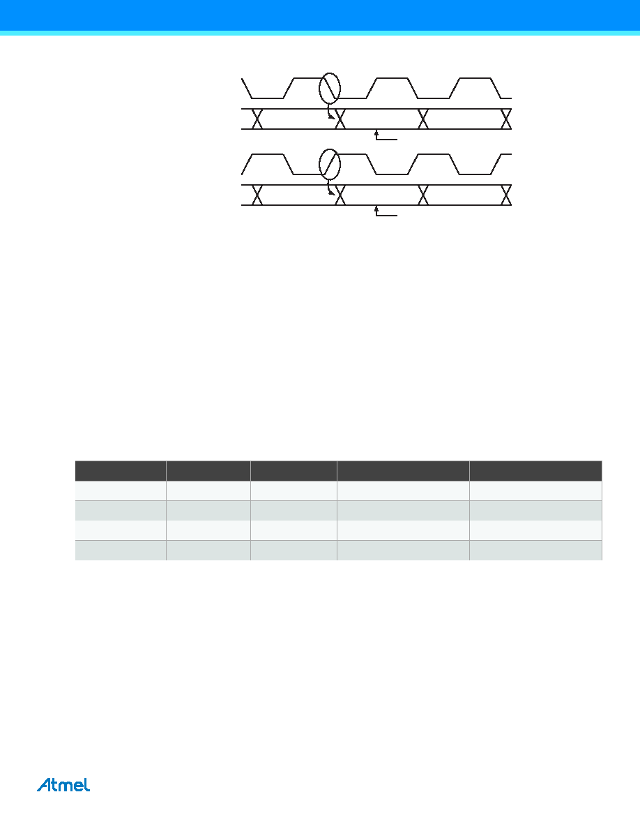
Figure 21-3. Synchronous mode XCK timing.
Using the inverted I/O (INVEN) setting for the corresponding XCK port pin, the XCK clock edges used for data sampling
and data change can be selected. If inverted I/O is disabled (INVEN=0), data will be changed at the rising XCK clock
edge and sampled at the falling XCK clock edge. If inverted I/O is enabled (INVEN=1), data will be changed at the falling
XCK clock edge and sampled at the rising XCK clock edge. For more details, see “I/O Ports” on page 132.
21.3.5 Master SPI Mode Clock Generation
For master SPI mode operation, only internal clock generation is supported. This is identical to the USART synchronous
master mode, and the baud rate or BSEL setting is calculated using the same equations (see Table 21-1 on page 233).
There are four combinations of the SPI clock (SCK) phase and polarity with respect to the serial data, and these are
determined by the clock phase (UCPHA) control bit and the inverted I/O pin (INVEN) settings. The data transfer timing
diagrams are shown in Figure 21-4 on page 236. Data bits are shifted out and latched in on opposite edges of the XCK
signal, ensuring sufficient time for data signals to stabilize. The UCPHA and INVEN settings are summarized in Table 21-
2 on page 235. Changing the setting of any of these bits during transmission will corrupt both the receiver and
transmitter.
Table 21-2. INVEN and UCPHA functionality.
The leading edge is the first clock edge of a clock cycle. The trailing edge is the last clock edge of a clock cycle.
RxD / TxD
XCK
RxD / TxD
XCK
UCPOL = 0
UCPOL = 1
Sample
SPI Mode
INVEN
UCPHA
Leading edge
Trailing edge
0
Rising, sample
Falling, setup
1
0
1
Rising, setup
Falling, sample
2
1
0
Falling, sample
Rising, setup
3
1
Falling, setup
Rising, sample
发布紧急采购,3分钟左右您将得到回复。
相关PDF资料
PIC18F4321T-I/ML
IC PIC MCU FLASH 4KX16 44QFN
PIC18F4221T-I/ML
IC PIC MCU FLASH 2KX16 44QFN
PIC18F2321T-I/ML
IC PIC MCU FLASH 4KX16 28QFN
PIC18F2221T-I/SO
IC PIC MCU FLASH 2KX16 28SOIC
PIC16LF1939-I/MV
IC MCU 8BIT 28KB FLASH 40-UQFN
PIC24F16KL402-I/SP
IC MCU 16BIT 16KB FLASH 28-SPDIP
PIC18F24J11-I/SS
IC PIC MCU FLASH 16K 2V 28-SSOP
PIC24F16KA101-I/SO
IC PIC MCU FLASH 16K 20-SOIC
相关代理商/技术参数
PIC18F4450T-I/PT
功能描述:8位微控制器 -MCU 16KB FL 768 RAM 34 I/O FS-USB 2.0 RoHS:否 制造商:Silicon Labs 核心:8051 处理器系列:C8051F39x 数据总线宽度:8 bit 最大时钟频率:50 MHz 程序存储器大小:16 KB 数据 RAM 大小:1 KB 片上 ADC:Yes 工作电源电压:1.8 V to 3.6 V 工作温度范围:- 40 C to + 105 C 封装 / 箱体:QFN-20 安装风格:SMD/SMT
PIC18F4455-BL
制造商:POWERLITE SYSTEMS 功能描述:PIC18F445 W/ BOOTLOADER FOR FLASHLAB 制造商:POWERLITE SYSTEMS 功能描述:PIC18F445 W/ BOOTLOADER, FOR FLASHLAB 制造商:POWERLITE SYSTEMS 功能描述:PIC18F445 W/ BOOTLOADER, FOR FLASHLAB; Silicon Manufacturer:Powerlite Systems; Core Architecture:PIC; Kit Contents:Board; Features:Bootloader Programming, RS232 Connector for Boot-Loading and Serial Comms ;RoHS Compliant: Yes
PIC18F4455-I/ML
功能描述:8位微控制器 -MCU 24kBF 2048RM FSUSB2 RoHS:否 制造商:Silicon Labs 核心:8051 处理器系列:C8051F39x 数据总线宽度:8 bit 最大时钟频率:50 MHz 程序存储器大小:16 KB 数据 RAM 大小:1 KB 片上 ADC:Yes 工作电源电压:1.8 V to 3.6 V 工作温度范围:- 40 C to + 105 C 封装 / 箱体:QFN-20 安装风格:SMD/SMT
PIC18F4455-I/P
功能描述:8位微控制器 -MCU 24kBF 2048RM FSUSB2 RoHS:否 制造商:Silicon Labs 核心:8051 处理器系列:C8051F39x 数据总线宽度:8 bit 最大时钟频率:50 MHz 程序存储器大小:16 KB 数据 RAM 大小:1 KB 片上 ADC:Yes 工作电源电压:1.8 V to 3.6 V 工作温度范围:- 40 C to + 105 C 封装 / 箱体:QFN-20 安装风格:SMD/SMT
PIC18F4455-I/PT
功能描述:8位微控制器 -MCU 24kBF 2048RM FSUSB2 RoHS:否 制造商:Silicon Labs 核心:8051 处理器系列:C8051F39x 数据总线宽度:8 bit 最大时钟频率:50 MHz 程序存储器大小:16 KB 数据 RAM 大小:1 KB 片上 ADC:Yes 工作电源电压:1.8 V to 3.6 V 工作温度范围:- 40 C to + 105 C 封装 / 箱体:QFN-20 安装风格:SMD/SMT
PIC18F4455T-I/ML
功能描述:8位微控制器 -MCU 24kBF 2048RM FSUSB2 RoHS:否 制造商:Silicon Labs 核心:8051 处理器系列:C8051F39x 数据总线宽度:8 bit 最大时钟频率:50 MHz 程序存储器大小:16 KB 数据 RAM 大小:1 KB 片上 ADC:Yes 工作电源电压:1.8 V to 3.6 V 工作温度范围:- 40 C to + 105 C 封装 / 箱体:QFN-20 安装风格:SMD/SMT
PIC18F4455T-I/PT
功能描述:8位微控制器 -MCU 24kBF 2048RM FSUSB2 RoHS:否 制造商:Silicon Labs 核心:8051 处理器系列:C8051F39x 数据总线宽度:8 bit 最大时钟频率:50 MHz 程序存储器大小:16 KB 数据 RAM 大小:1 KB 片上 ADC:Yes 工作电源电压:1.8 V to 3.6 V 工作温度范围:- 40 C to + 105 C 封装 / 箱体:QFN-20 安装风格:SMD/SMT
PIC18F4458-I/ML
功能描述:8位微控制器 -MCU 24KB Flash 2KB RAM RoHS:否 制造商:Silicon Labs 核心:8051 处理器系列:C8051F39x 数据总线宽度:8 bit 最大时钟频率:50 MHz 程序存储器大小:16 KB 数据 RAM 大小:1 KB 片上 ADC:Yes 工作电源电压:1.8 V to 3.6 V 工作温度范围:- 40 C to + 105 C 封装 / 箱体:QFN-20 安装风格:SMD/SMT